May 8, 2025
Smart Polygons: Advanced PCB Design Just Got Easier
Share
BuildWithFlux


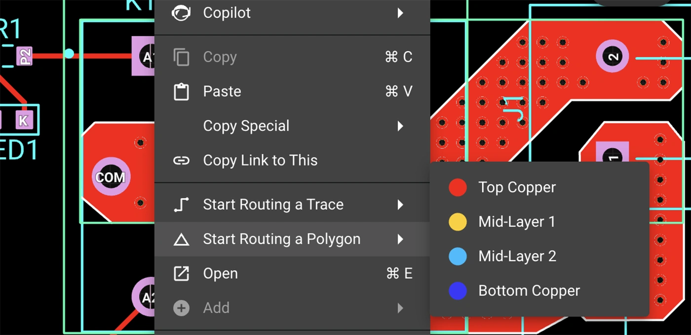
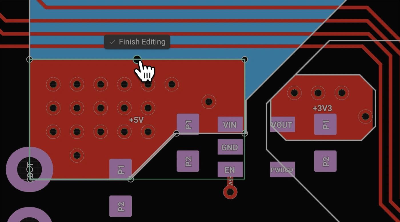
Smart Polygons in Flux behave intuitively like traces, making them straightforward to learn and use—start directly from any pad with automatic net association, simply click to place and adjust points, and watch as copper intelligently reflows in real-time. Let’s dive in!
In PCB design, polygons are customizable copper shapes directly tied to a specific net. They’re crucial because they significantly influence the electrical performance and reliability of your PCB. Polygons allow you to optimize your board layout for specific electrical properties, including improved grounding, controlled impedance, and efficient heat distribution.
Specifically, polygons are indispensable for:
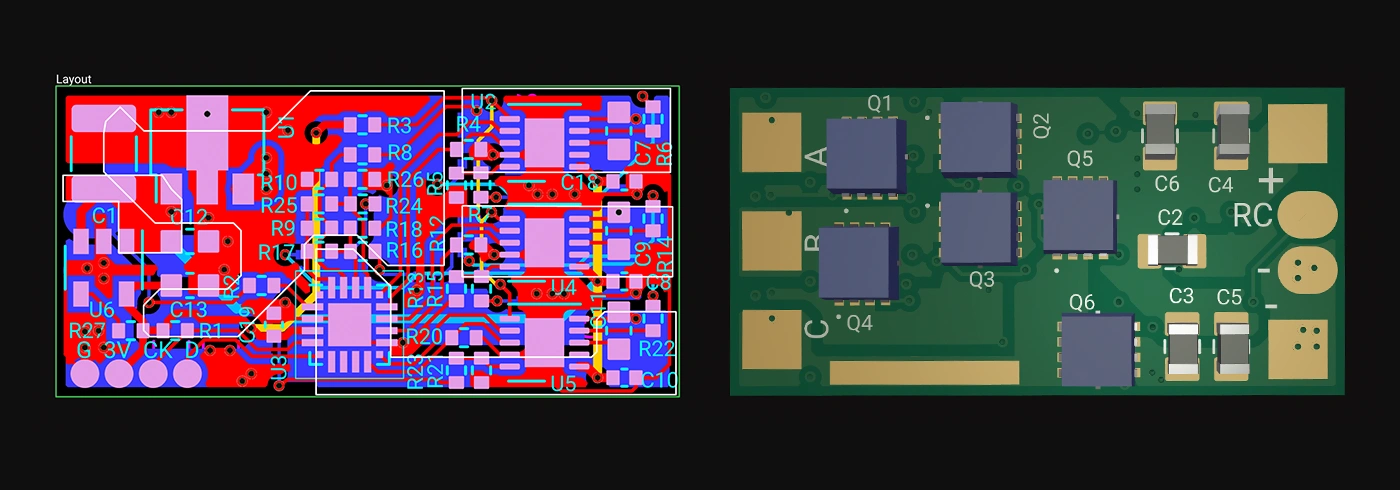
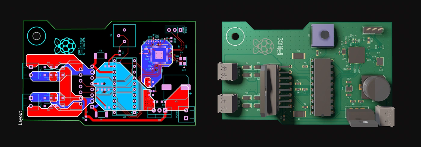
{{polygons-examples}}
Unlike zones—which define areas where copper cannot exist—polygons actively conduct electricity and shape your board's electrical performance, making them fundamental for advanced PCB designs.
At Flux, we prioritize intuitive, user-friendly workflows. Automatic copper fills were the first step. Now with polygons, we've continued this approach:
Polygons in Flux behave intuitively like traces, making them straightforward to learn and use, right from the start.
Polygons in Flux pack powerful functionality without complexity:
Polygons unlock new possibilities in your PCB designs. Here are a few practical ways you'll benefit:
Whether you're just dipping your toes into PCB design or you’re a veteran engineer tackling complex layouts, polygons in Flux offer the ideal balance of simplicity and capability:
Polygons are available now in Flux, ready to enhance your PCB design capabilities. Explore this powerful feature today and experience firsthand how advanced design can truly be this easy.
Dive in now and check out our detailed polygon documentation or jump straight into Flux to try it yourself. We can't wait to hear what you think!
Smart Polygons in Flux behave intuitively like traces, making them straightforward to learn and use—start directly from any pad with automatic net association, simply click to place and adjust points, and watch as copper intelligently reflows in real-time. Let’s dive in!
In PCB design, polygons are customizable copper shapes directly tied to a specific net. They’re crucial because they significantly influence the electrical performance and reliability of your PCB. Polygons allow you to optimize your board layout for specific electrical properties, including improved grounding, controlled impedance, and efficient heat distribution.
Specifically, polygons are indispensable for:
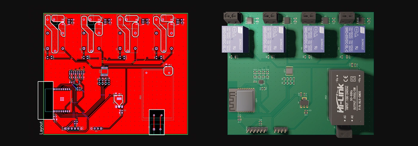
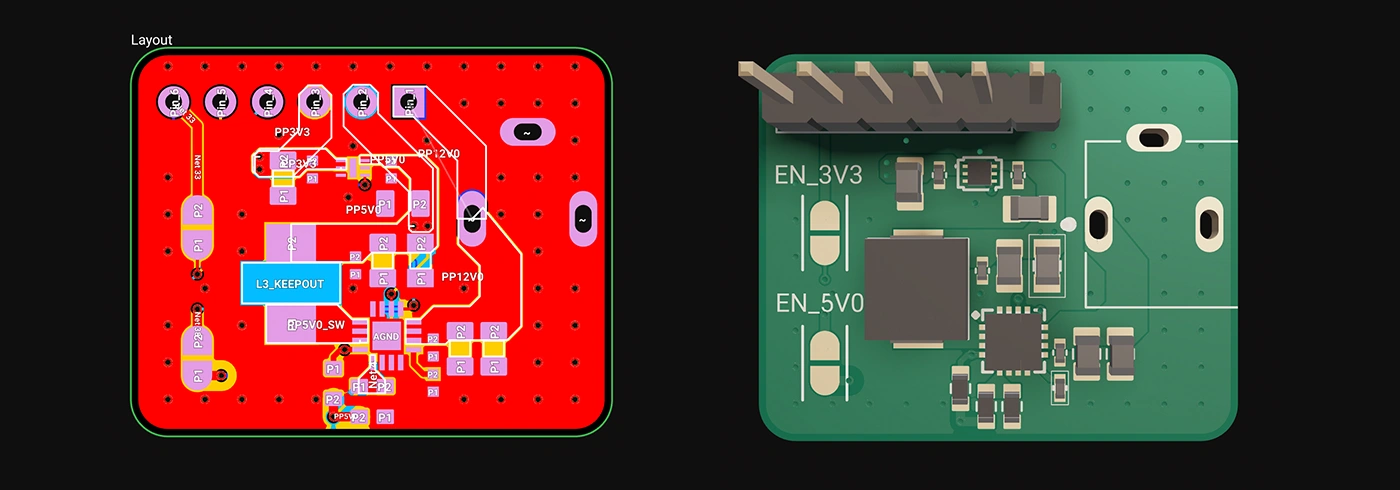
{{polygons-examples}}
Unlike zones—which define areas where copper cannot exist—polygons actively conduct electricity and shape your board's electrical performance, making them fundamental for advanced PCB designs.
At Flux, we prioritize intuitive, user-friendly workflows. Automatic copper fills were the first step. Now with polygons, we've continued this approach:
Polygons in Flux behave intuitively like traces, making them straightforward to learn and use, right from the start.
Polygons in Flux pack powerful functionality without complexity:
Polygons unlock new possibilities in your PCB designs. Here are a few practical ways you'll benefit:
Whether you're just dipping your toes into PCB design or you’re a veteran engineer tackling complex layouts, polygons in Flux offer the ideal balance of simplicity and capability:
Polygons are available now in Flux, ready to enhance your PCB design capabilities. Explore this powerful feature today and experience firsthand how advanced design can truly be this easy.
Dive in now and check out our detailed polygon documentation or jump straight into Flux to try it yourself. We can't wait to hear what you think!


If you're a lover of smart home devices, you're likely buzzing with excitement over Arduino's recent collaboration with Silicon Labs. We are too, and we’re even more excited to bring the power of this collaboration to life on Flux. As of today, we’re excited to announce that engineers can fully design Arduino-based Matter boards with Flux.
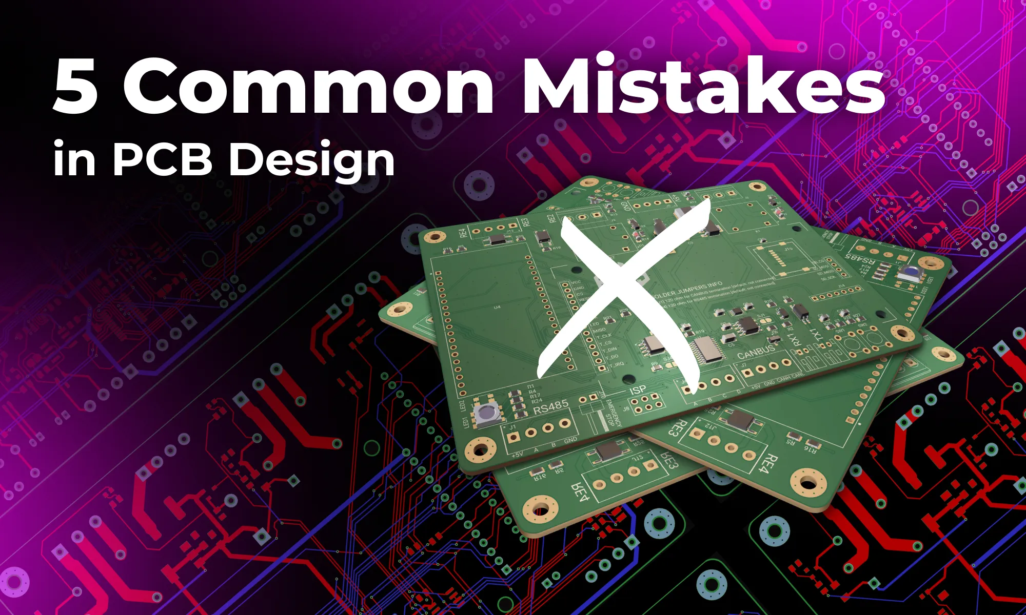
Avoid costly errors in your PCB design with these expert tips! Discover the 5 most common mistakes in trace width, vias, power planes, and more. Learn how Flux’s AI Copilot helps you catch these issues early, ensuring your board is ready for manufacturing.
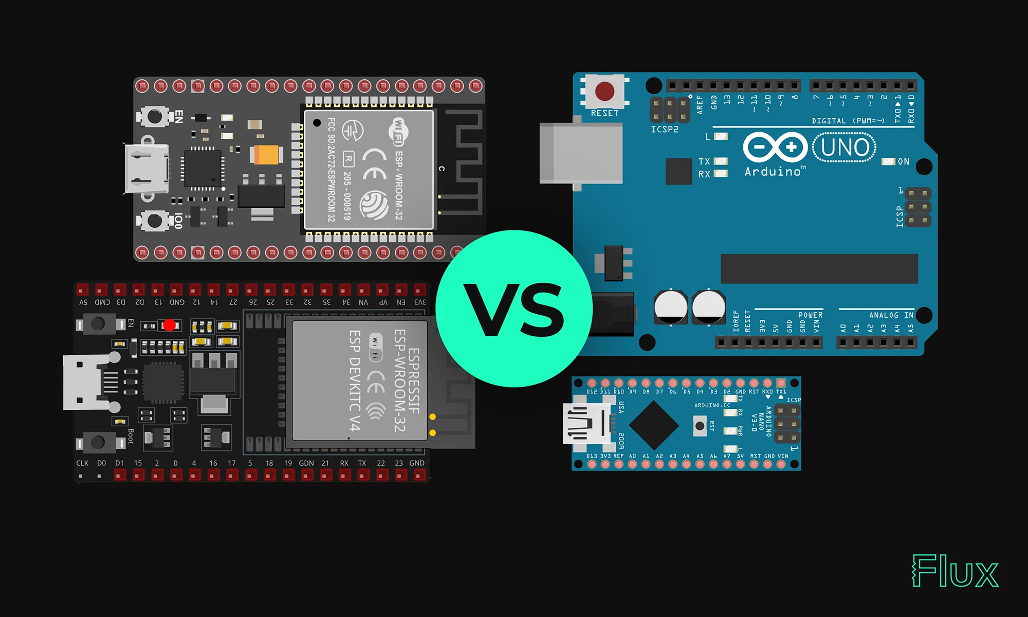
Our 2023 guide compares ESP32 and Arduino, two essential microcontrollers in IoT. ESP32 offers advanced features like Wi-Fi, while Arduino excels in ease of use and community support. Choose based on your project's complexity and needs.

Delve into the essentials of circuit diagrams, exploring the various electronics symbols and their roles in design, while also offering practical advice for effective use of diagramming tools like Flux.

If you're looking to improve your understanding of schematic diagrams, this article is the perfect starting point. Let's explore the crucial role of circuits and components schematics in translating conceptual electrical designs into physical printed circuit board assemblies (PCBAs).

ESP32 microcontrollers are affordable, low-power SoCs with integrated Wi-Fi and Bluetooth. Offering dual-core processing, ample memory, and versatility, they excel in IoT, wearables, and smart home applications. The ESP32's continuous evolution promises exciting possibilities ahead.

We’ve been so amazed with the ways you’ve used Copilot to brainstorm, debug, and conduct part research that we’ve compiled some of our favorite prompts you can copy and paste, or modify for your own use!

Today, we’re launching automatic photorealistic 3D renderings so that you can put your best foot forward and share your work to the world. Now, anyone can effortlessly create stunning, dynamic, and professional 3D renders.
Discover how Flux.ai enhanced its web app performance using the open-source tool, log-time-to-next-idle. The blog details how to measure user interactions and pinpoint their completion point for optimal performance. Learn from our experience and apply these strategies to refine your app's user experience.
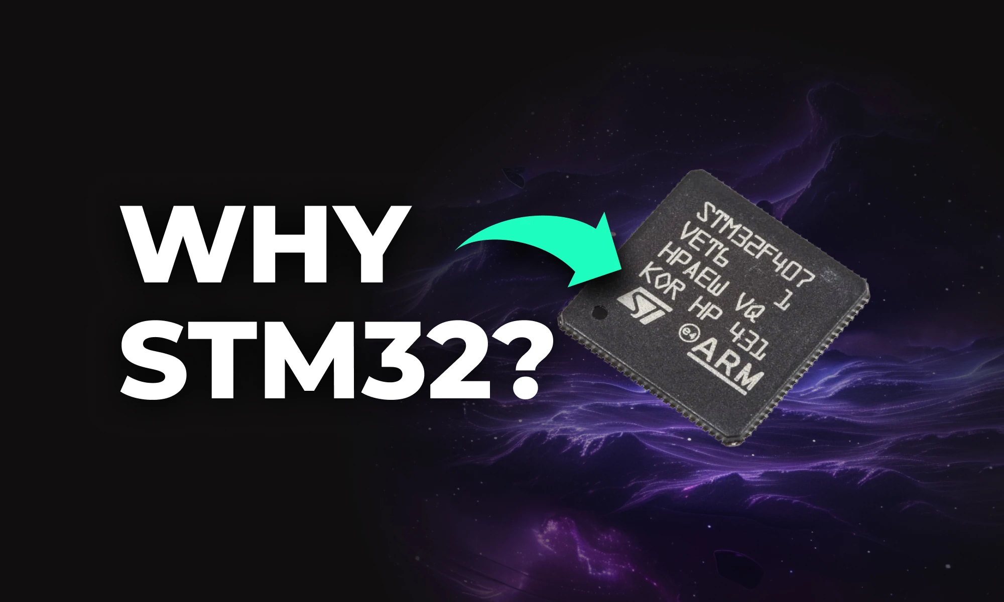
Learn about STM32 microcontrollers, popular series, USB OTG, SWD, UART, and development tools. Find the right STM32 MCU and kickstart your projects.

The guide provides an easy-to-follow formula for converting mm to mils, essential in engineering and PCB design for precise measurements and applications.

One of the key components of PCBs are vias, which are tiny pathways that allow electrical signals to travel from one layer of the board to another. Vias are a staple of PCB design.